Researchers move a step closer to making conventional optoelectronic devices more lightweight and flexible.
In organic optoelectronic devices, the control of molecular deposition on thin films is important for optimal surface arrangement and device performance. In a recent study, researchers developed a new method for achieving stable deposition on thin films effectively. They also developed a tool to track real-time potential changes on the surface. These findings are expected to aid the improvement of organic devices, such as organic light-emitting diodes, in terms of efficacy and durability.

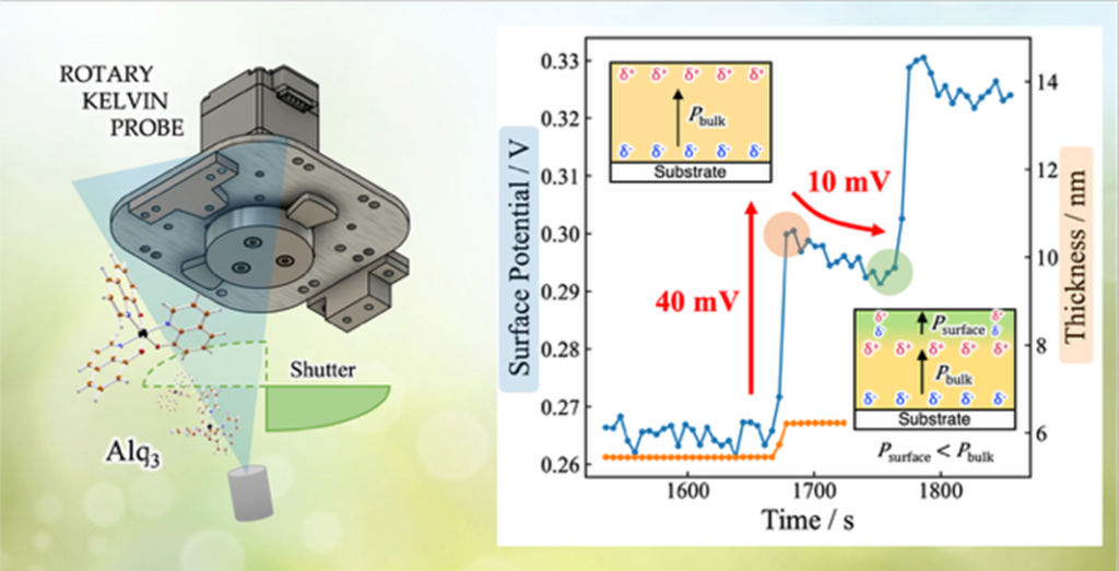
Image title: A schematic of the apparatus developed for the vacuum deposition method.
Image caption: The primary component of the rotary Kelvin probe features a rotary electrode and its surroundings. Additionally, it shows the vacuum deposition system, with a crucible and a computer-controlled shutter.
Image credit: Prof. Hisao Ishii of Chiba University, Japan
License type: Original content
Usage restrictions: Cannot be reused without permission.
Organic optoelectronic devices, such as organic light-emitting diodes (OLEDs), use molecules with specific structures arranged on thin films. Additionally, the arrangement of these molecules on any surface is crucial for various processes that occur within these devices. This arrangement is guided by two primary factors: the deposition rate (how fast the molecules are placed) and the surface temperature. Slower deposition rates and higher temperatures facilitate the proper arrangement, resulting in more stable structures. Finding the right time scale for this process is also critical, and researchers are now looking for ways to control these factors for optimal molecular arrangement on surfaces.
In a new study, a team from Japan led by Prof. Hisao Ishii from the Graduate School of Science and Engineering and the Center for Frontier Science at Chiba University, along with Masahiro Ohara from Chiba University and Dr. Yuya Tanaka from the Graduate School of Science and Technology at Gunma University, has introduced a new method of deposition that achieves suitable molecular arrangement. The article was made available online on December 4, 2023, and published in Volume 15, Issue 49 of the journal ACS Applied Materials and Interfaces on December 13, 2023. “When depositing organic molecules by vacuum deposition, the orientation of the molecules is changed over time by pausing the deposition. Moreover, by changing the deposition conditions, it is possible to invert the orientation of both the head- and tail-end of the molecules,” explains Prof. Ishii.
In their study, the team found a simple yet ingenious way to control the orientation of molecules deposited on aluminum and benzene-containing thin films, denoted as Alq3 and TPBi, respectively. They used a method called “intermittent deposition,” which introduces breaks during the deposition process, and developed an updated version of a tool called “rotary Kelvin probe” (RKP). This was used to measure the surface potential (voltage on the material’s surface) during and after the deposition in real-time. By repeatedly opening and closing the deposition shutter at specific intervals, the researchers could change the polarization (the distribution of charges), influencing how the molecules were oriented on the films.
The new approach of intermittent deposition created a relaxed and stable surface layer with controllable polarization. The study also revealed how surface relaxation affected molecular orientation and the formation of a potential valley (shaped like a “V”). In fact, this deposition method enables the creation of an arbitrary potential profile for desired molecular orientations on the thin film of interest.
In terms of applications, this intermittent deposition technique can enhance the effectivity and lifetime of OLED materials. In addition, it can also be used for non-polar organic molecules, making it useful for devices like organic photovoltaic cells and transistors. Prof. Ishii emphasizes, “This method is expected to further improve the efficiency and lifetime of OLEDs. Beyond OLEDs, it also promotes the development of other organic devices, such as organic memory devices. Therefore, replacing conventional inorganic devices with organic devices will make lightweight and flexible devices readily available.”
In summary, this study explores the relaxation processes that impact the orientation of molecules on the surface of organic thin films and utilizes intermittent deposition to create a stable surface layer effectively. Additionally, an RKP tool is developed to analyze changes in surface potential over time. The proposed deposition method is expected to work with various organic molecules (not just polar ones) and could pave the way for the improvement of existing organic devices and the development of new ones.
About Professor Hisao Ishii
Dr. Hisao Ishii is a Professor at the Graduate School of Science and Engineering and the Center for Frontier Science and Molecular Chirality Research Center at Chiba University, Japan. He obtained his Ph.D. from the University of Tokyo in 1991 and specializes in organic electronics with over 13,000 citations and 250 publications. He has won several awards, including a Best Paper Award from the Surface Science Society of Japan (2010), a research award from the Japan OLED forum (2009), and the 13th fellow award from the Japan Society of Applied Physics (2019). He also holds memberships in organizations like The Surface Science Society of Japan and The Chemical Society of Japan.
Funding:
This research was supported by the Japan Society for the Promotion of Science (JSPS)
KAKENHI Grant-in-Aid for Scientific Research (grant nos. 20H02810 and 21K05208) and Grant-in-Aid for JSPS Fellows (grant no. 22J21883).
Reference:
| Title of original paper: | Impact of Intermittent Deposition on Spontaneous Orientation Polarization of Organic Amorphous Films Revealed by Rotary Kelvin Probe |
| Authors: | Masahiro Ohara1, Hokuto Hamada1, Noritaka Matsuura1, Yuya Tanaka2, and Hisao Ishii1,3 |
| Affiliations: |
|
| Journal: | ACS Applied Materials and Interfaces |
| DOI: | 10.1021/acsami.3c12914 |
Contact: Hisao Ishii
Professor, Graduate School of Science and Engineering, Chiba University
Email: ishii130@faculty.chiba-u.jp
Public Relations Office, Chiba University
Address: 1-33 Yayoi, Inage, Chiba 263-8522 JAPAN
Email: koho-press@chiba-u.jp
Tel: +81-43-290-2018
Recommend
-

Touchable Buddha Project: Bridging Heritage and 3D Technology for Community Revitalization through Design
2024.03.29
-

Reassessing the role of “Forest Resources” in achieving carbon neutrality: Measuring forests with the combination of drones, mathematics, and computer graphics
2023.09.12
-

Interdisciplinary Collaborations to Solve Social Issues: Frontier Bioresearch at Chiba University
2023.03.17


